As semiconductor processes advance toward 5nm nodes and below, equipment positioning accuracy requirements have transitioned from the "micron level" to the "sub-nanometer level." Conventional electromagnetic actuators, limited by mechanical backlash and response delays, are gradually unable to meet the stringent demands of advanced processes. Piezoelectric actuators, leveraging their inherent advantages based on the inverse piezoelectric effect, are delivering nanometer-scale resolution and microsecond-level response times, establishing themselves as the key technological foundation enabling the semiconductor industry to pursue smaller linewidths and higher yields.
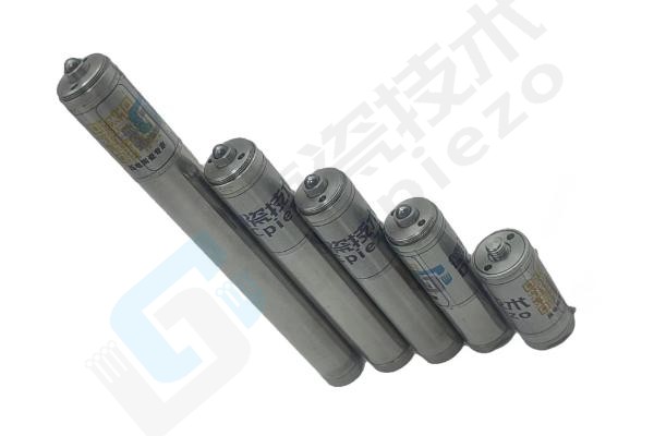
I. From Principle to Advantages: Why Is Piezoelectric Technology the Fab's Top Choice?
Piezoelectric actuators, operating on the electrostrictive effect of piezoelectric materials (such as PZT ceramics and piezoelectric single crystals), achieve direct, lossless conversion from electrical to mechanical energy. Compared to conventional solutions, their core advantages directly address the pain points of semiconductor manufacturing:
●Nanometer-Level Positioning Accuracy: Displacement resolution can reach below 0.1 nanometers, providing a physical guarantee for lithography alignment.
●Microsecond-Level Dynamic Response: Eliminates the inductive delays of electromagnetic coils, meeting the demands of high-speed scanning and rapid stepping.
●Backlash-Free Direct Drive: Eliminates transmission structures, fundamentally removing mechanical backlash and friction wear.
●Closed-Loop Integration Capability: Built-in displacement sensors enable in-situ real-time feedback, ensuring long-term stability.
II. Front-End Core Processes: How Does Piezoelectric Technology Support Lithography and Etching?
In front-end semiconductor manufacturing, piezoelectric actuators have become indispensable components in critical equipment such as lithography scanners and etchers.
●Lithography Wafer Stage and Reticle Stage – Coarse/Fine Composite Actuation
In dual-stage systems, piezoelectric actuators work in concert with linear motors: the linear motor handles large-stroke rapid motion, while the piezoelectric actuator takes care of fine end-stage compensation. Their cooperation compresses stage positioning errors to within 1 nanometer, providing robust support for overlay accuracy at 7nm nodes and below.
●Projection Lens Focusing and Reticle Correction
To address minor wafer surface warpage or equipment thermal drift, piezoelectric actuators integrated into the lens module can perform real-time nanoscale axial adjustments, ensuring exposure focus is always locked at the optimal focal plane. Meanwhile, actuators on the reticle side can respond quickly to compensate for pattern distortion caused by thermal expansion, safeguarding pattern transfer fidelity.
●Wafer Attitude Fine-Tuning in Etch and Deposition Chambers
In plasma etching and CVD processes, piezoelectric actuators are embedded into the electrostatic chuck base, dynamically adjusting wafer surface levelness and flatness within milliseconds. This effectively improves plasma distribution uniformity, controlling the etch rate difference between the wafer edge and center to minimal levels, significantly enhancing within-chip critical dimension uniformity.
III. Back-End Packaging and Inspection: Precision Protection from Bonding to Handling
The packaging stage also demands extreme precision, where piezoelectric actuators play critical roles in chip interconnection and automated operations.
●Flip-Chip Bonding and Wire Bonding – Micro-Bump Alignment
Piezoelectric actuators drive the bonding head to achieve high-precision alignment between micro-bumps and substrate pads, controlling alignment accuracy at the 0.5 nanometer level, ensuring high-density I/O packaging reliability. Simultaneously, bonding force is precisely controlled in real-time via the piezoelectric element, ensuring adequate weld strength while preventing over-pressure damage to the chip's fragile low-k dielectric layers.
●Ultrasonic Transduction and Force Control
The ultrasonic vibration required for wire bonding is stably delivered by piezoelectric transducers at tens of kilohertz, significantly improving intermetallic bonding quality between gold/copper wires and pads.
●Wafer Handling and Pre-Alignment
Ultra-thin wafers are highly susceptible to micro-cracks during robotic end-effector pick-up. Flexible clamping mechanisms integrated with piezoelectric tactile feedback can sense subtle changes in contact force, enabling damage-free handling of thin and warped wafers, significantly reducing breakage rates.
IV. Advancing Toward More Advanced Nodes: The Self-Evolution of Piezoelectric Technology
To keep pace with the continued scaling of semiconductor processes, piezoelectric actuators themselves are undergoing rapid iteration:
●Application of Single-Crystal Piezoelectric Materials: Compared with traditional PZT polycrystalline ceramics, displacement output capacity is increased by over 30%, while response speed further breaks through the microsecond barrier.
●Enhanced Closed-Loop Stability: Smart actuators integrated with nanometer-level displacement sensors achieve long-term drift suppression improvement exceeding 50%, significantly reducing equipment downtime for recalibration.
●Low-Heat and Cleanroom Compatibility: Drive power consumption continues to decrease, with heat generation and electromagnetic interference significantly reduced, fully compliant with semiconductor fabs' stringent thermal stability and cleanliness requirements.
From nanoscale positioning of lithography stages to precise micro-bump alignment in bonders, piezoelectric actuators have become deeply integrated throughout the entire semiconductor manufacturing chain. With the continued proliferation of EUV lithography and the ramp-up of 3D advanced packaging volume production, the market demand for faster, smaller, and more robust piezoelectric solutions will only intensify. Guangdong Deci Technology Co., Ltd. remains dedicated to the R&D and manufacturing of multilayer stack piezoelectric ceramics, leveraging superior material properties and customization capabilities to help semiconductor clients worldwide overcome precision actuation barriers and win together in the new era of advanced manufacturing.




24小时免费咨询
请输入您的联系电话,座机请加区号